Boys with their toys
What goes on in the lab when working on Bitfold
These are the times when almost none of the electronic devices available to consumers can be dismantled and repaired, as it was 20 years ago. Over time, we got used to treating them like boxes where magic happens. It doesn’t matter what magic it is, as long as it works. Meanwhile, these are usually sophisticated products of engineering thought, over which many months or even years were spent in laboratories.
It’s all the same with Bitfold.
Like ogres, devices have layers
Even the most complex in its design, every electronic appliance has similar major components. First, it requires a power source to operate. Then memory to store and retrieve data. Another is the microprocessor – a small integrated circuit that process information as the ‘brain’ of the device. Furthermore, most devices use a communication interface such as Wi-Fi, Bluetooth, or USB to connect to other devices or networks.
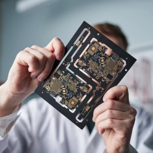
And finally – PCB. This just have layers! You can see it when you glimpse at one from the side. Printed circuit boards (PCBs) are used to connect many various parts within a device and provide a platform for all the circuits. Let’s stop here for several reasons.
Stories have layers as well
First of all, it is because of PCBs that we now have our own laboratory in Bitfold with such a kind of equipment. Nothing probably would have worked out if it wasn’t for the lab. You can read a bit about our journey in the previous blog post.
Further, to fit all components on only one PCB was the most arduous in case of Biftold. The desired device was intended not to exceed the dimensions of a smartphone, so it had to be relatively small. No doubt, these are the challenges that engineers like the most.
Finally – and perhaps most importantly – the specific architecture of Bitfold PCB is where the whole story began. Due to our patented hardware solution, not only 3 processors had to fit on the board, but also one additional digital circuit, which our engineers used to call ‘processor number four’. Sounds intriguing, right? This will be addressed yet in a moment, please stay patient.
Here comes the eminence grise
To imagine how essential it is, a PCB can be loosely compared to designing a city. While fabrication can be likened to setting the paths, streets, and zoning of a city, the assembly of components is placing buildings, housing estates and common facilities in a predetermined order on this well-thought-out grid.
Moving away from urban associations, a printed circuit board may also resemble the nervous system of a human or animal. Just as nerve tissue is responsible for transmitting signals between different parts of our body, conductive paths on a PCB allow electronic signals to flow between different electronic components. To put it simple – it allows the device to function as a whole and keeps the inside together.
The fourth element
Now let it be revealed. The previously mentioned mysterious circuit that our PCB also has to carry is a hardware air-gap. Combined with FPGA (field-programmable gate array), often used in security-critical applications, it provides reliable protection against cyber threats.
An air-gap separates two independent Bitfold modules by a logic barrier, to prevent any unauthorized data transfer between them. To illustrate this, let’s use an example from nature again. Close to this concept is the way human’s circulatory system is organized. There are valves in our veins that prevent the backflow of blood, which is essential for maintaining the health and function of the body. Similarly, air-gapping protects against flow in the undesirable direction – from an unsecure system everywhere outside to a secure one requiring the utmost care.
This isolation ensures that even if one of Bitfold’s system is compromised, the other system remains protected. And it can’t be emphasized enough – this is exactly what will soon allow you to transact directly from your Bitfold whilst your private keys are kept offline all the time. Ta-da!
The great gathering
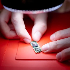
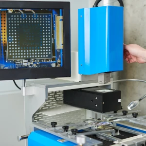
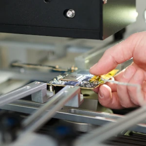
Now let’s check how working on it looks like every day. As soon as ready-to-assemble PCBs reach Bitfold laboratory, two eye-catching machines awaits to do their precise part of the task. These are the pick-and-place machine and the BGA station. The first one is used to accurately place relatively small surface-mounted components on solder paste previously applied on it in a method similar to the screen-printing technique.
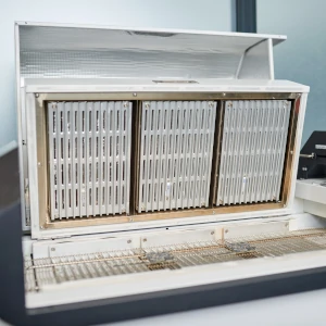
Once all the components are in place, it’s time for the soldering oven, used to reflow the solder paste. After the board is placed in, the oven preheats it to melt the paste, creating a permanent electrical connection between the components and the board.
The second machine – BGA station – is generally used to fix any shortcomings in the process described above. It mounts components with small solder balls on their bottom (ball grid array – BGA) that the station melts when attaching.
Dotting the i’s and crossing the t’s
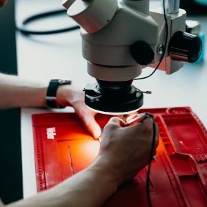
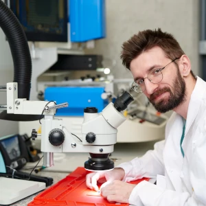
It becomes really accurate to juxtapose the nervous system with the PCB’s role when you notice that our engineers also have a microscope at their disposal at Bitfold laboratory. It provides a detailed view of the surface of the board and the components, allowing technicians to identify any issue that may affect the functionality or reliability of the board.
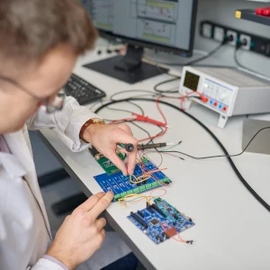
Now the time has come to introduce probably the most expensive Bitfold’slab equipment – PXI. Named from PCI eXtensions for Instrumentation, it is a platform that allows for quick and convenient connection of all kinds of electronic equipment with software.
At Bitfold, the PXI is used as a digital twin of the whole Bitfold platform. Thanks to digital modules, it is possible to effectively test new hardware solutions in isolation from dependent, physical subsystems. This allows for faster prototyping of new solutions as well as their integration and testing in any configuration of physical and digital modules.
The playground is open
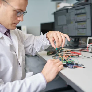
There are some other advanced devices in our lab that our engineers use every day to create Bitfold. We are constantly recruiting for the positions of programmers, electronics engineers, and testers in our company. Take a look at the “jobs” section and submit your application so that, like the rest of our team, you can play with the powerful toys that our laboratory is equipped with.
See you in the team!